Hardware FAQ
This page gathers all kinds of information we know about the PB hardware
CPU
- ARM
- Cirrus Logic EP7312 (Maverick)
- 74MHz
- 2x 16550 UART (serial)
- LCD display controller
- Datasheet
- User's Guide
Microcontroller
- 8052
- 24MHz
- 8052 Specs
- Headunit interfacing
- Datasheet (Winbond W78E516B)
- Winbond Chip Specs at 8052.com
D/A-Converter
- Cirrus Logic CS4341
- 16-bit
- Datasheet
or
- Burr-Brown/TI PCM1748E (U7)
- 24-bit/96kHz
- Datasheet
IDE interface controller
Flash ROM
- ST Micro M29W200BB (Flash ID 0020 0057)
- 2 MBit
- Automotive grade
- Datasheet
or
- AMD AM29LV200BB-90EC (Flash ID 0001 22BF)
- 2 MBit
- Commercial grade (0-70 degC)
- Datasheet
or
- Fujitsu MBM29LV200BC (Flash ID 0004 22BF)
- Datasheet
or
- Fujitsu MBM29LV400BC (Flash ID 0004 22BA)
- Datasheet
- Note: This is a 4 megabit chip, whereas all of the other ones are 2 megabit -- but it doesn't seem to matter...
or
- Silicon Storage Technology (SST) SST39VF200A (Flash ID 00BF 2789)
- Datasheet
Connection to CPU
The flash chip is connected to the ARM CPU for only 16 bit accesses (the nBYTE pin on the flash appears to be shorted to Vcc).
Flash address lines A[0:14], A[15] are connected to CPU address lines A[2:16], A[1]. A[0] on the CPU is not connected to the flash, thus also preventing byte-wise access.
The data lines appear to be connected straight-through.
Complex Programmable Logic Device (CPLD)
Power Regulator
- TDA3681J : Multiple voltage regulator with switch and ignition buffer [PHILIPS]
- Datasheet
The pins go from 1 to 17 from left to right as you're looking from the inside of the phatbox towards the back.
Constant Power Pins
- Pin 13 is ground
- Pin 15 (Regulator 2) should be 5V. This powers the microcontroller.
These pins should be on at least when the ignition is on, but don't require the head unit to be "on."
Switched Power Pins
- Pin 4 (Regulator 4) is 3.3V, This is the supply for the ARM, SDRAM, Flash, etc. (Enable input is pin 9.)
- Pin 2 (Regulator 3) is 5V (Enable input is pin 10.)
- Pin 1 (Regulator 1) is 8.5V, and I'm not sure it gets used for anything (it might not even be enabled, I haven't checked) (Enable input is pin 10.)
The regulators that supply the power on these pins are controlled by the 8051 and are only on when the PB is powered-up by the head unit.
PCB Layout (Photos)
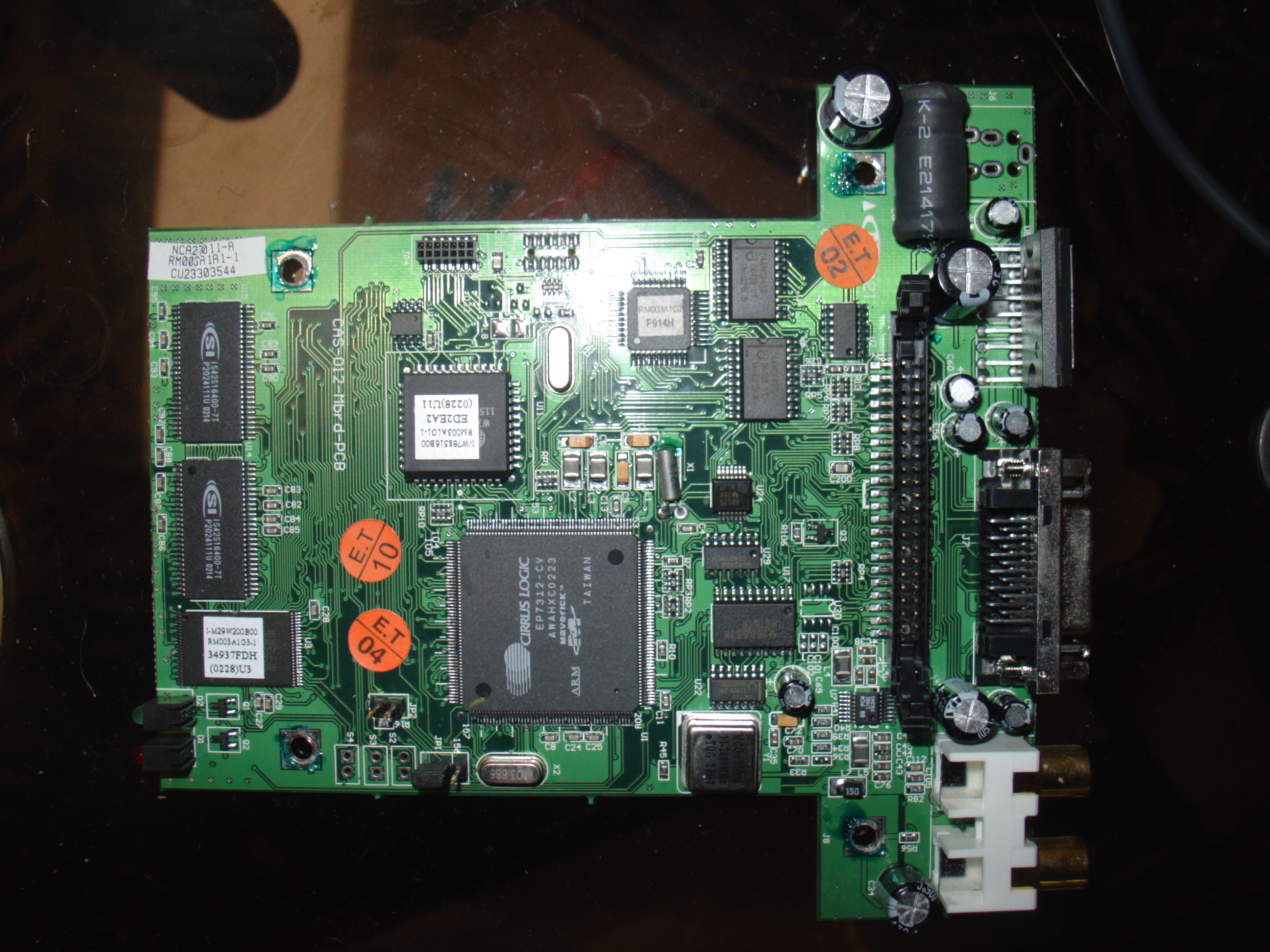
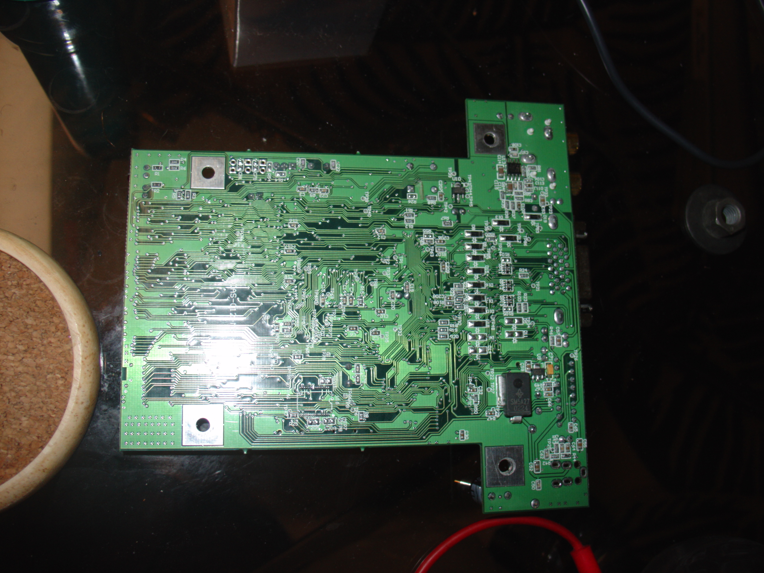
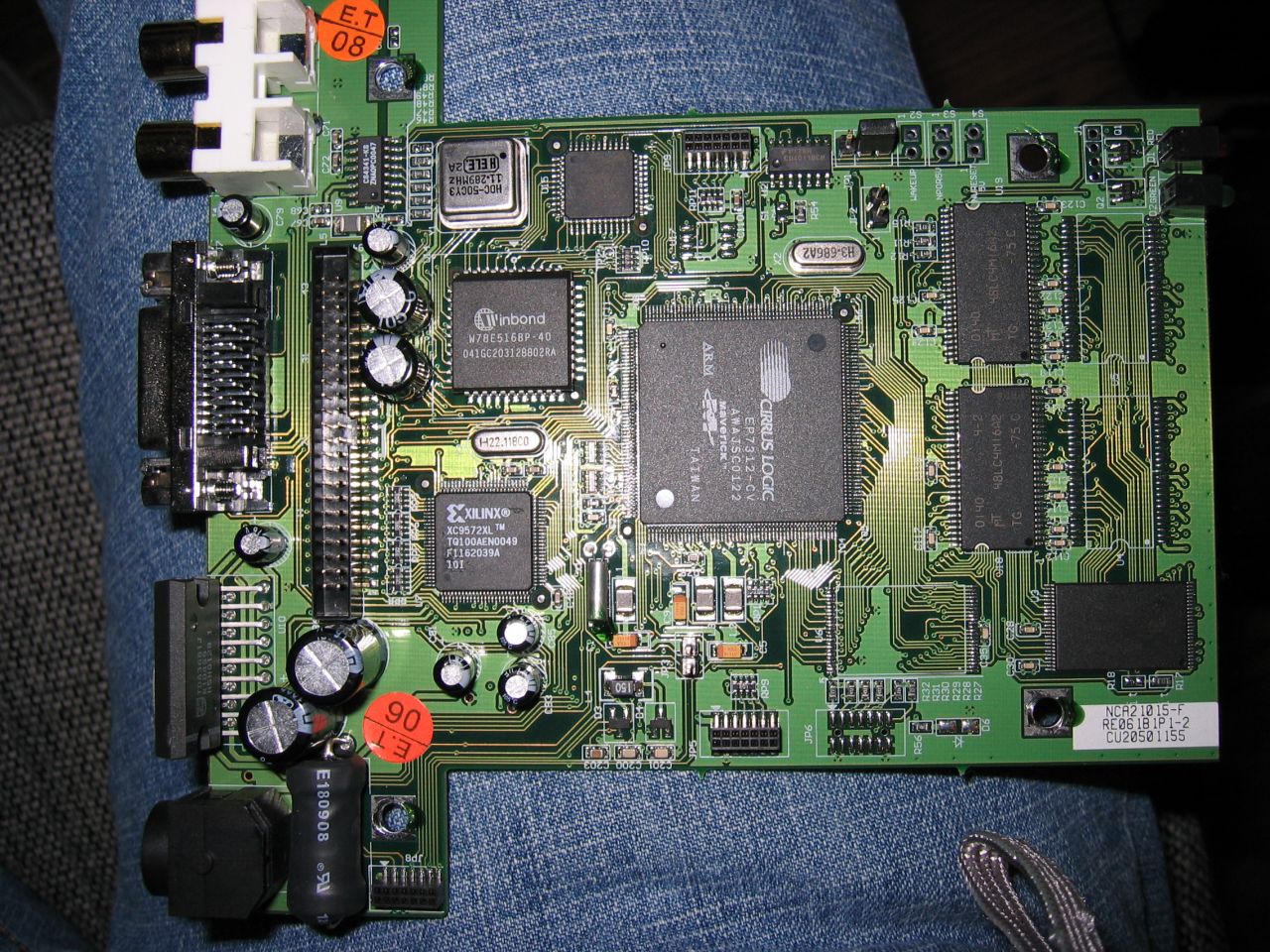
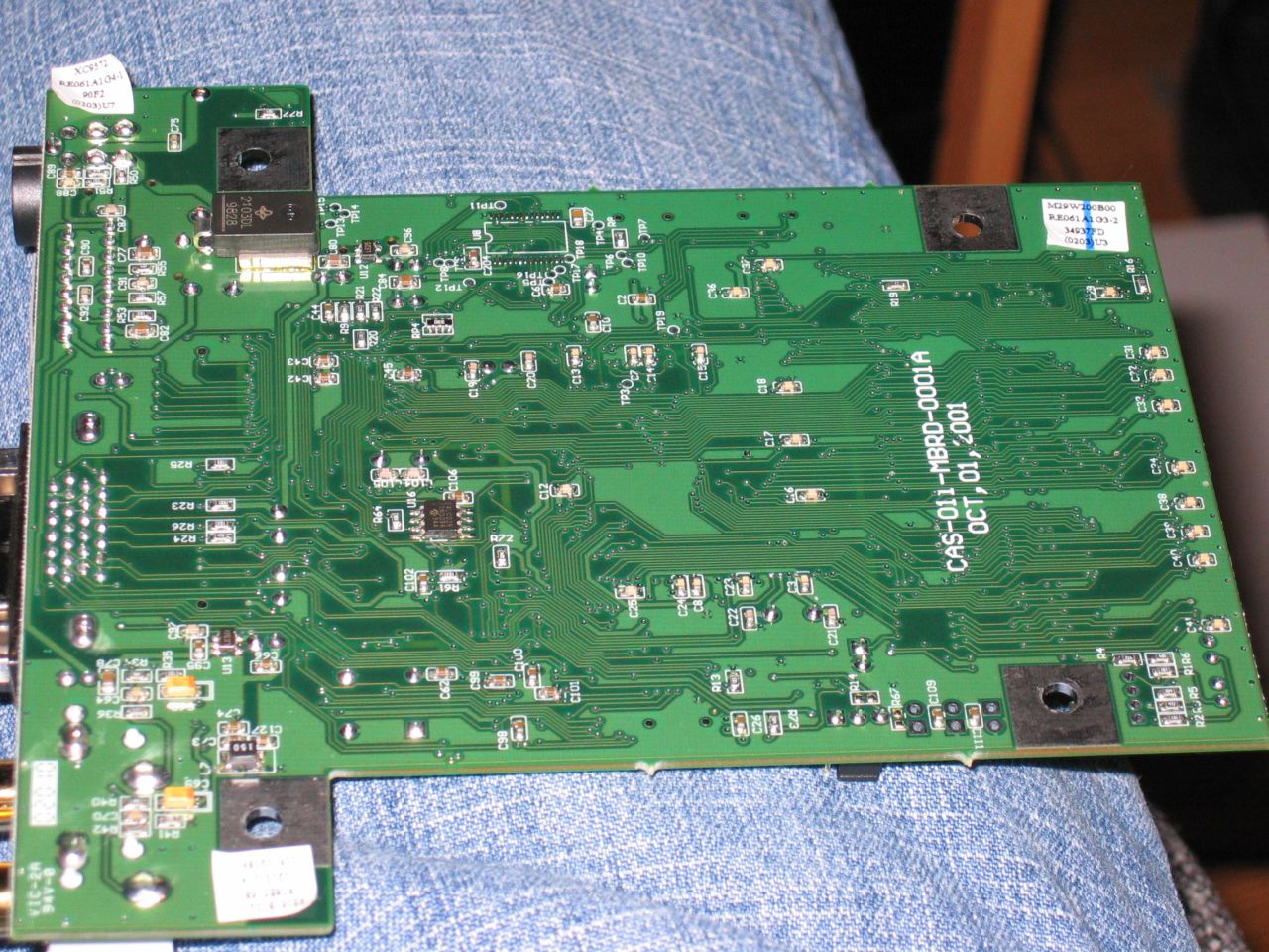
PCB Jumpers
JP1
- JP1 -- Power-on jumper?
- The center pin of this 3-pin block is connected to pins 9 and 10 of the voltage regulator -- that is to say, applying power to it causes the rest of the box to turn on.
- The box will not boot with no jumper.
- Some have had luck getting an apparently "dead" PhatBox to respond by either switching the jumper to its other position, or even just removing it and reinstalling it, while power was applied to the unit.
JP5
- JP5 -- XILINX 9572XL - JTAG
- Pin 6 > 9572XL Pin 48 - TCLK
- Pin 8 > 9572XL Pin 83 - TDO
- Pin 10 > 9572XL Pin 45 - TDI
- Pin 12 > 9572XL Pin 47 - TMS
JP6
- JP6 -- ARM JTAG (No Connector, just pads)
- Pin 3 > 7312 Pin 125 - nTRST
- Pin 5 > 7312 Pin 11 - TDI
- Pin 7 > 7312 Pin 58 - TMS
- Pin 9 > 7312 Pin 90 - TCLK
- Pin 11 > 7312 Pin 22 - TDO
JP8
This is JP4 on the C710 board
- JP8 -- ARM UART1 (SERIAL PORT!!!)
- Pin 1 > board power
- Pin 2 > pin18 - PB2 [GPIO port B]
- Pin 3 > some resistor, hard to trace past.
- Pin 5 > 7312 Pin 32 - TDX[1]
- Pin 7 > 7312 Pin 36 - RXD[1]
- Pin 9 > 7312 Pin 37 - DCD
- Pin 11 > 7312 Pin 38 - DSR
- Pin 13 > 7312 Pin 35 - CTS
JP9
- JP9 -- XILINX 5032C - JTAG
- Pin 6 > 5032C Pin 26 - TCLK
- Pin 8 > 5032C Pin 32 - TDO
- Pin 10 > 5032C Pin 1 - TDI
- Pin 12 > 5032C Pin 7 - TMS
For connections to the JP arrays you can use either: Molex 87332-1420 or DigiKey WM18078-ND
DMS Cartridge
- 2.5" Notebook harddisk (9.5mm, "rugged" edition)
- FAT32 filesystem
- 2 Partitions (PHTSYS, PHTDATA)